Hardware DIY Construction Manual for STM32C011J6 (SO8 case)
A Veroboard compatible PCB layout is described for the STM32C011J6 (SO8 case) processor.
Because it is complicated to etch PCBs without appropriate tools, a simple Veroboard compatible PCB layout is presented here. Because such a layout is quite coarse, also etching is possible with simple equipment. An appropriate TIF file is available for download.
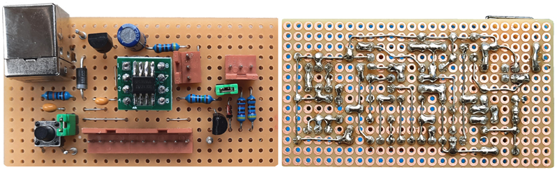
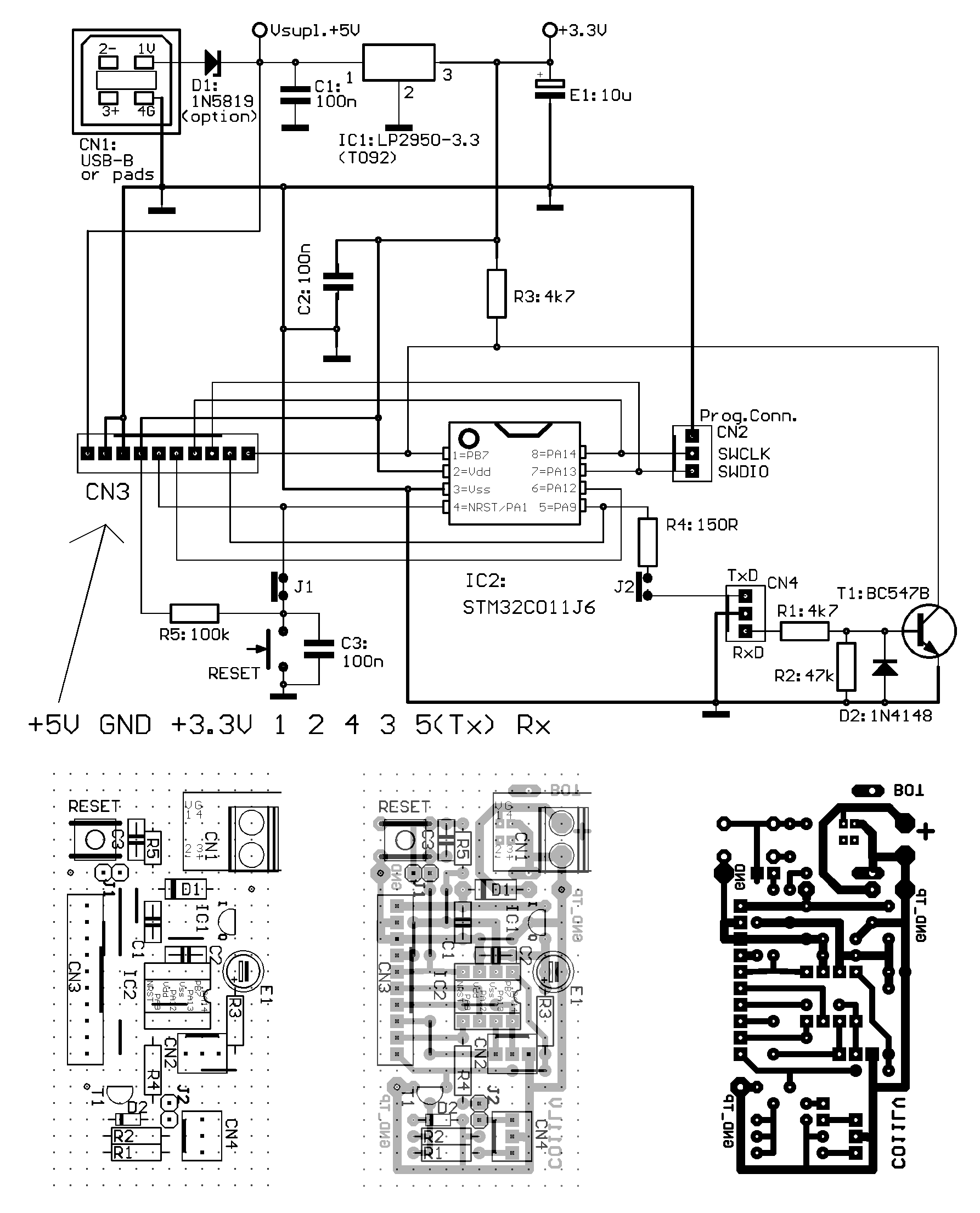
The proposed Veroboard compatible PCB layout is made of three parts: left hand standard power connector and manual reset button, middle the processor kernel and user I/O, right hand the terminal interface.
BOTTOM layer as well as component placement view are "from component side", i.e. BOTTOM layer shown mirrored "through the PCB" (as needed for PCB production). The documented PCB size is a little bit larger than necessary. Cut off as needed.
Veroboard layout:
For easy handling of common power supplies, an USB-B socket is installed on the prototype. But pads for simple solder wiring are provided on the PCB,too. Diode D1 may be shorted, if 5V power is supplied from a standard USB power supply, but may be secure when any experimental power is supplied.
Special parts: (cited suppliers are examples where private consumers can buy in Germany)
---STM32C011J6M6: Reichelt, tme.eu, Mouser et.al.
Don't confuse with STM32C011J4M6, has only 16kB Flash !
---SO8 to DIL8 breakout board: Reichelt BB SOP8.
---RS-232 and programmer connector: source Reichelt PS 25/3G BR or Conrad 741221
---10 pin peripheral connector: source Reichelt PS 25/10G BR Conrad 741264
Recommended drill diameters for etched PCB:
resistors, capacitors, diodes, transistor, ICs, jumper wires 0.8mm; CN2, CN3, CN4, Diode D1 and GND test pins 1.0mm
USB socket: 0.8mm/metal flag 2.0mm or 1.0mm+jigsaw slit
Hints for Veroboard assembly
It is useful to print a mirrored version of the placement drawing to get a view from bottom=solder side.
The diameter of the wire should be 0.5 or 0.4 mm for easy bending and diagonal wiring between the neighboured copper dots. A set of "adjustment" pliers with small flat tips (or stable tweezers) is recommended for bending and positioning the wires. For 45 degree bendings, a small screw driver pressed on the wire is helpful.
The correct positioning of parts is essential, because there is almost no reserve for alternative positioning. The final solder process is less complicated than it looks. So it is recommended first to place all parts (bigger and typical parts first) and solder them as slightly as possible only to fix them provisionally. Next cut longer wires of fixed components about 1 mm above the Veroboard for later final soldering. At this stage, parts with more than two contacts like connectors should be soldered only at 2 diagonal edge pins. Try to organize the solder sequence in a way that one alreay soldered point is connected with another yet unsoldered, if possible. Points wit 2.5 mm distance are not soldered with a wire, but with a dot of solder instead. If you are connecting points with 3.6 or 5mm distance, becareful not to unsolder the already soldered point due to much heat on the wire.
contact: wschemmert@t-online.de, www.midi-and-more.de
* Right of technical modifications reserved. Provided 'as is' - without any warranty. Any responsibility is excluded.
* This description is for information only. No product specifications are assured in juridical sense.
* Trademarks and product names cited in this text are property of their respective owners.